
Today’s 200mm wafer production demands reliable, accurate and fast wafer probing solutions. Our 200mm automated wafer probers are based on the production-proven Horizon platform to meet these demands for high-volume, low-cost manufacturing, as well as leading-edge, multi-die and bumped wafer applications.
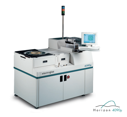
The 4090µ+, our top 200mm prober, is available as an upgrade to 4080, 4090, and 4090µ probers to extend the advanced applications of your 200mm tools and maximize your investment!
Key features and available upgrades of our EG 4000 series Horizon probers are;
- Probe camera optics and an advanced vision system greatly increase probe card alignment speed.
- Accuracy up to +/-3µ for 4090µ+.
- Supports 4″, 6″, and 8″ wafers in both thin and standard thicknesses.
- High Voltage testing upgrades, for testing power products.
- MicroTouch™, a technology that allows probers to delicately control the speed of Z motion for handling Cu and Low K Dielectric devices.
- Closed Loop handler upgrades, for improved reliability.
- Scripted scrub and brush upgrades for cleaning probe needles while the machine is automatically running, keeping throughput high without reducing yield.
- Thermal Agility, our term designating probers with the ability to quickly heat up or cool down the chuck top between -55°C and 155°C for temperature testing.
Which system is right for you?
- EG4090µ+
- EG4090µ+ Fast Probe
Unprecedented productivity for volume 200mm wafer manufacturing
For chipmakers that want to maximize their investment in 200mm test equipment, accurate and reliable high-volume probing is more important than ever. The 4090µ+ is designed to meet these demands while reducing test costs through increased throughput, simplified operation and state-of-the-art automation.
4090µ+ Key Benefits:
The ability to address the testing demands associated with fine-pitch devices, copper interconnects, low-k dielectrics and other advanced applications. Reduced pad damage with MicroTouch. Decreased test costs by increasing test cell availability and throughput. Simplified, efficient operation through “one-button” probing and self-calibration features. Increased probe card alignment speed and accuracy by utilizing advanced vision system and probe camera optics.The 4090µ+ is also available as an upgrade to 4080, 4090, and 4090µ probers to extend the advanced applications of your 200mm tools and maximize your investment.
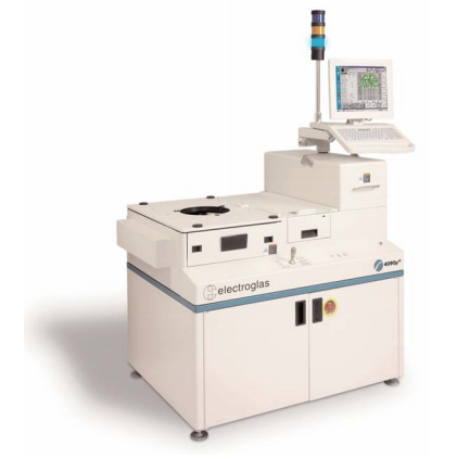
Fast Probing for High Throughput of Small Die
For many chipmakers engaged in 200mm wafer production, throughput is the single most important factor with regard to wafer probing. The Horizon 4090µ+ Fast Probe is designed to meet the need for speed, delivering the shortest 200 mm wafer probing stepping times available.
4090µ+ Fast Probe Key Benefits:
- Increased manufacturing throughput and productivity.
- Reduced cost-of-ownership for applications that require short test times or testing of large numbers of die per wafer.
- 40-50 percent gain in system throughput and manufacturing for low-cost, commodity-type devices.